Integrated circuit
A monolithic integrated circuit (also known as IC, microchip, silicon chip, computer chip or chip) is a miniaturized electronic circuit (consisting mainly of semiconductor devices, as well as passive components) that has been manufactured in the surface of a thin substrate of semiconductor material. A hybrid integrated circuit is a miniaturized electronic circuit constructed of individual semiconductor devices, as well as passive components, bonded to a substrate or circuit board. This article is about monolithic integrated circuits.
Integrated Circuits can be found in almost every electronic device today. Anything, from a common wristwatch to a personal computer has Integrated Circuits in it. There are circuits that control almost everything, as simple as a temperature control in a common iron or a clock in a microwave oven. This has made a major difference in how we operate electronic items. Not only does it make electronic items simpler to use, for example, on most microwave ovens now, you have preset controls for different settings. Now you can push a button and it will automatically set the time for defrosting an item or popping popcorn.
In the future, Integrated circuits may even be used for medical purposes. For example, Research has been going on since the late 1980s in which they are trying to develop a computer chip that can be attached to the brain to repair different types of brain damage. With this kind of link, they would be able to repair some kinds of blindness or even memory loss from brain damage.
Only a half-century after their development was initiated, integrated circuits can be found everywhere. Computers, cellular phones, and other digital appliances are now entangled parts of the structure of modern technological societies. In other words, modern computing, communications, manufacturing, and transport systems, including the Internet, all depend on the existence of integrated circuits. Indeed, many scholars believe that the digital revolution that is based on integrated circuits is one of the most significant developments in the history of mankind.
Introduction
Integrated circuits were made possible by experimental discoveries showing that semiconductor devices could perform the functions of vacuum tubes, and by mid-twentieth-century technology advancements in semiconductor device fabrication. The integration of large numbers of tiny transistors into a small chip was an enormous improvement over the manual assembly of circuits using discrete electronic components. The integrated circuit's mass production capability, reliability, and building-block approach to circuit design ensured the rapid adoption of standardized ICs in place of designs using discrete transistors.
There are two main advantages of ICs over discrete circuits: cost and performance. Cost is low because the chips, with all their components, are printed as a unit by photolithography and not constructed one transistor at a time. Performance is high, because the components are small, close together, switch quickly, and consume little power. As of 2006, chip areas range from a few square millimeters (mm2) to around 250 mm2, with up to 1 million transistors per mm2.
Advances in integrated circuits
Among the most advanced integrated circuits are the microprocessors, that control everything from computers to cellular phones to digital microwave ovens. Digital memory chips are another family of integrated circuit that is crucially important to the modern information society. While the cost of designing and developing a complex integrated circuit is quite high, when spread across typically millions of production units the individual IC cost is minimized. The performance of ICs is high because the small size allows short traces which in turn allows low power logic (such as CMOS) to be used at fast switching speeds.
ICs have consistently migrated to smaller feature sizes over the years, allowing more circuitry to be packed on each chip. This increased capacity per unit area can be used to decrease cost and/or increase functionality. Moore's law, in its modern interpretation, states that the number of transistors in an integrated circuit doubles every two years. In general, as the feature size shrinks, almost everything improves—the cost-per-unit and the switching power consumption go down, and the speed goes up. However, ICs with nanometer-scale devices are not without their problems, principal among which is leakage current, although these problems are not insurmountable and will likely be improved by the introduction of high-k dielectrics. Since these speed and power consumption gains are apparent to the end user, there is fierce competition among manufacturers to use finer geometries. This process, and the expected progress over the next few years, is well described by the International Technology Roadmap for Semiconductors (ITRS).
Classification
Integrated circuits can be classified into analog, digital and mixed signal (both analog and digital on the same chip).
Digital integrated circuits can contain anything from one to millions of logic gates, flip-flops, multiplexers, and other circuits in a few square millimeters. The small size of these circuits allows high speed, low power dissipation, and reduced manufacturing cost compared with board-level integration. These digital ICs, typically microprocessors, digital signal processors (DSPs), and microcontrollers work using binary mathematics to process "one" and "zero" signals.
Analog ICs, such as sensors, power-management circuits, and operational amplifiers work by processing continuous signals. They perform functions like amplification, active filtering, demodulation, mixing, etc. Analog ICs ease the burden on circuit designers by having expertly designed analog circuits available instead of designing a difficult analog circuit from scratch.
ICs can also combine analog and digital circuits on a single chip to create functions such as analog-to-digital converters and digital-to-analog converters. Such circuits offer smaller size and lower cost, but must carefully account for signal interference.
Manufacture
Fabrication
The semiconductors of the periodic table of the chemical elements were identified as the most likely materials for a solid state vacuum tube by researchers like William Shockley at Bell Laboratories starting in the 1930s. Starting with copper oxide, proceeding to germanium, then silicon, the materials were systematically studied in the 1940s and 1950s. Today, silicon monocrystals are the main substrate used for integrated circuits (ICs) although some III-V compounds of the periodic table such as gallium arsenide are used for specialized applications like LEDs, lasers, and the highest-speed integrated circuits. It took decades to perfect methods of creating crystals without defects in the crystalline structure of the semiconducting material.
Semiconductor ICs are fabricated in a layer process which includes these key process steps:
- Imaging
- Deposition
- Etching
The main process steps are supplemented by doping, cleaning and planarisation steps.
Mono-crystal silicon wafers (or for special applications, silicon on sapphire or gallium arsenide wafers) are used as the substrate. Photolithography is used to mark different areas of the substrate to be doped or to have polysilicon, insulators or metal (typically aluminum) tracks deposited on them.
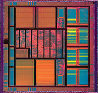
- For a CMOS process, for example, a transistor is formed by the criss-crossing intersection of striped layers. The stripes can be monocrystalline substrate, doped layers, perhaps insulator layers or polysilicon layers. Some etched vias to the doped layers might interconnect layers with metal conducting tracks.
- The criss-crossed checkerboard-like (see image above) transistors are the most common part of the circuit, each checker forming a transistor.
- Resistive structures, meandering stripes of varying lengths, form the loads on the circuit. The ratio of the length of the resistive structure to its width, combined with its sheet resistivity determines the resistance.
- Capacitive structures, in form very much like the parallel conducting plates of a traditional electrical capacitor, are formed according to the area of the "plates," with insulating material between the plates. Owing to limitations in size, only very small capacitances can be created on an IC.
- More rarely, inductive structures can be simulated by gyrators.
Since a CMOS device only draws current on the transition between logic states, CMOS devices consume much less current than bipolar devices.
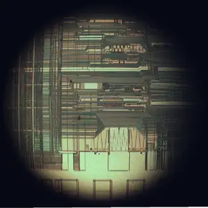
A (random access memory) is the most regular type of integrated circuit; the highest density devices are thus memories; but even a microprocessor will have memory on the chip. (See the regular array structure at the bottom of the first image.) Although the structures are intricate—with widths which have been shrinking for decades—the layers remain much thinner than the device widths. The layers of material are fabricated much like a photographic process, although light waves in the visible spectrum cannot be used to "expose" a layer of material, as they would be too large for the features. Thus photons of higher frequencies (typically ultraviolet) are used to create the patterns for each layer. Because each feature is so small, electron microscopes are essential tools for a process engineer who might be debugging a fabrication process.
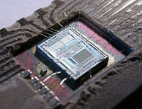
Each device is tested before packaging using very expensive automated test equipment (ATE), a process known as wafer testing, or wafer probing. The wafer is then cut into small rectangles called dice. Each good die (N.B. die is the singular form of dice, although dies is also used as the plural) is then connected into a package using aluminum (or gold) wires which are welded to pads, usually found around the edge of the die. After packaging, the devices go through final test on the same or similar ATE used during wafer probing. Test cost can account for over 25 percent of the cost of fabrication on lower cost products, but can be negligible on low yielding, larger, and/or higher cost devices.
As of 2005, a fabrication facility (commonly known as a semiconductor fab) costs over a billion US Dollars to construct, because much of the operation is automated. The most advanced processes employ the following specifications:
- The wafers are up to 300 mm in diameter (wider than a common dinner plate).
- Use of 90 nanometer or smaller chip manufacturing process. Intel, IBM, and AMD are using 90 nanometers for their CPU chips, and Intel has started using a 65 nanometer process.
- Copper interconnects where copper wiring replaces aluminum for interconnects.
- Low-K dielectric insulators.
- Silicon on insulator (SOI)
- Strained silicon in a process used by IBM known as Strained silicon directly on insulator (SSDOI)
Packaging
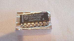
The earliest integrated circuits were packaged in ceramic flat packs, which continued to be used by the military for their reliability and small size for many years. Commercial circuit packaging quickly moved to the dual in-line package (DIP), first in ceramic and later in plastic. In the 1980s, pin counts of VLSI circuits exceeded the practical limit for DIP packaging, leading to pin grid array (PGA) and leadless chip carrier (LCC) packages. Surface mount packaging appeared in the early 1980s and became popular in the late 1980s, using finer lead pitch with leads formed as either gull-wing or J-lead, as exemplified by Small-Outline Integrated Circuit. A carrier which occupies an area about 30 percent – 50 percent less than an equivalent DIP, with a typical thickness that is 70 percent less. This package has "gull wing" leads protruding from the two long sides and a lead spacing of 0.050 inches.
Small-Outline Integrated Circuit (SOIC) and PLCC packages. In the late 1990s, PQFP and TSOP packages became the most common for high pin count devices, though PGA packages are still often used for high-end microprocessors. Intel and AMD are currently transitioning from PGA packages on high-end microprocessors to land grid array (LGA) packages.
Ball grid array (BGA) packages have existed since the 1970s.
Traces out of the die, through the package, and into the printed circuit board have very different electrical properties, compared to on-chip signals. They require special design techniques and need much more electric power than signals confined to the chip itself.
When multiple die are put in one package, it is called SiP, for System In Package. When multiple die are combined on a small substrate, often ceramic, it's called a MCM, or Multi-Chip Module. The boundary between a big MCM and a small printed circuit board is sometimes fuzzy.
History, origins, and generations
Birth of the IC
The integrated circuit was first conceived by a radar scientist, Geoffrey W.A. Dummer (born 1909), working for the Royal Radar Establishment of the British Ministry of Defence, and published in Washington, D.C. on May 7, 1952. Dummer unsuccessfully attempted to build such a circuit in 1956.
The first integrated circuits were manufactured independently by two scientists: Jack Kilby of Texas Instruments and Robert Noyce of Fairchild Semiconductor. Kilby filed a patent application for a "Solid Circuit" made of germanium on February 6, 1959. Kilby received several patents: U.S. patent 3138743 , U.S. patent 3138747 , U.S. patent 3261081 , and U.S. patent 3434015 . (See Chip that Jack built[1].) Noyce was awarded a patent for a more complex "unitary circuit" made of silicon on April 25, 1961. He credited Kurt Lehovec of Sprague Electric for a key concept behind the IC: the principle of p-n junction isolation by the action of a biased p-n junction (the diode).[2]
===SSI, MSI, LSI===
The first integrated circuits contained only a few transistors. Called "Small-Scale Integration" (SSI), they used circuits containing transistors numbering in the tens.
SSI circuits were crucial to early aerospace projects, and vice-versa. Both the Minuteman missile and Apollo program needed lightweight digital computers for their inertially-guided flight computers; the Apollo guidance computer led and motivated the integrated-circuit technology, while the Minuteman missile forced it into mass-production.
These programs purchased almost all of the available integrated circuits from 1960 through 1963, and almost alone provided the demand that funded the production improvements to get the production costs from $1,000/circuit (in 1960 dollars) to merely $25/circuit (in 1963 dollars). They began to appear in consumer products at the turn of the decade, a typical application being FM inter-carrier sound processing in television receivers.
The next step in the development of integrated circuits, taken in the late 1960s, introduced devices which contained hundreds of transistors on each chip, called "Medium-Scale Integration" (MSI).
They were attractive economically because while they cost little more to produce than SSI devices, they allowed more complex systems to be produced using smaller circuit boards, less assembly work (because of fewer separate components), and a number of other advantages.
Further development, driven by the same economic factors, led to "Large-Scale Integration" (LSI) in the mid 1970s, with tens of thousands of transistors-per-chip.
LSI circuits began to be produced in large quantities around 1970, for computer main memories and pocket calculators.
VLSI
The final step in the development process, starting in the 1980s and continuing on, was "Very Large-Scale Integration" (VLSI), with hundreds of thousands of transistors, and beyond (well past several million in the latest stages).
For the first time it became possible to fabricate a CPU on a single integrated circuit, to create a microprocessor. In 1986, the first one megabit Random Access Memory (RAM) chips were introduced, which contained more than one million transistors. Microprocessor chips produced in 1994 contained more than three million transistors.
This step was largely made possible by the codification of "design rules" for the CMOS technology used in VLSI chips, which made production of working devices much more of a systematic endeavor. (See the 1980 landmark text by Carver Mead and Lynn Conway referenced below.)
ULSI, WSI, SOC
To reflect further growth of the complexity, the term ULSI that stands for "Ultra-Large Scale Integration" was proposed for chips of complexity more than 1 million of transistors. However there is no qualitative leap between VLSI and ULSI, hence normally in technical texts the "VLSI" term covers ULSI as well, and "ULSI" is reserved only for cases when it is necessary to emphasize the chip complexity, e.g. in marketing.
The most extreme integration technique is wafer-scale integration (WSI), which uses whole uncut wafers containing entire computers (processors as well as memory). Attempts to take this step commercially in the 1980s (for instance, by Gene Amdahl) failed, mostly because of defect-free manufacturability problems, and it does not now seem to be a high priority for industry.
The WSI technique failed commercially, but advances in semiconductor manufacturing allowed for another attack on IC complexity, known as System-on-Chip (SOC) design. In this approach, components traditionally manufactured as separate chips to be wired together on a printed circuit board are designed to occupy a single chip that contains memory, microprocessor(s), peripheral interfaces, Input/Output logic control, data converters, and other components, together composing the whole electronic system.
Other developments
In the 1980s programmable integrated circuits were developed. These devices contain circuits whose logical function and connectivity can be programmed by the user, rather than being fixed by the integrated circuit manufacturer. This allows a single chip to be programmed to implement different LSI-type functions such as logic gates, adders, and registers. Current devices named FPGAs (Field Programmable Gate Arrays) can now implement tens of thousands of LSI circuits in parallel and operate up to 400 MHz.
The techniques perfected by the integrated circuits industry over the last three decades have been used to create microscopic machines, known as MEMS. These devices are used in a variety of commercial and military applications. Examples of commercial applications include DLP projectors, inkjet printers, and accelerometers used to deploy automobile airbags.
In the past, radios could not be fabricated in the same low-cost processes as microprocessors. But since 1998, a large number of radio chips have been developed using CMOS processes. Examples include Intel's DECT cordless phone, or Atheros's 802.11 card.
Silicon Graffiti
Ever since ICs were created, some chip designers have used the silicon surface area for surreptitious, non-functional images or words. These are sometimes referred to as Chip Art, Silicon Art, Silicon Graffiti, or Silicon Doodling.
Key industrial and academic data
Notable ICs
- The 555 common multivibrator subcircuit (common in electronic timing circuits)
- The 741 operational amplifier
- 7400 series TTL logic building blocks
- 4000 series, the CMOS counterpart to the 7400 series
- Intel 4004, the world's first microprocessor
- The MOS Technology 6502 and Zilog Z80 microprocessors, used in many home computers
Manufacturers
A list of notable manufacturers; some operating, some defunct:
- Agere Systems (formerly part of Lucent, which was formerly part of AT&T)
- Agilent Technologies (formerly part of Hewlett-Packard, spun-off in 1999)
- Alcatel
- Allegro Microsystems
- Altera
- AMD (Advanced Micro Devices; founded by ex-Fairchild employees)
- Analog Devices
- ATI Technologies (Array Technologies Incorporated; acquired parts of Tseng Labs in 1997)
- Atmel (co-founded by ex-Intel employee)
- Broadcom
- Commodore Semiconductor Group (formerly MOS Technology)
- Cypress Semiconductor
- Fairchild Semiconductor (founded by ex-Shockley Semiconductor employees: the "Traitorous Eight")
- Freescale Semiconductor (formerly part of Motorola)
- GMT Microelectronics (formerly Commodore Semiconductor Group)
- Hitachi
- IBM (International Business Machines)
- Infineon Technologies (formerly part of Siemens)
- Intel (founded by ex-Fairchild employees)
- Intersil (formerly Harris Semiconductor)
- Lattice Semiconductor
- Linear Technology
- LSI Logic (founded by ex-Fairchild employees)
- Maxim IC
- Marvell Technology Group
- MicroSystems International
- MOS Technology (founded by ex-Motorola employees)
- Mostek (founded by ex-Texas Instruments employees)
- National Semiconductor (aka "NatSemi"; founded by ex-Fairchild employees)
- Nordic Semiconductor (formerly known as Nordic VLSI)
- NEC Corporation (formerly known as Nippon Electric Company)
- NVIDIA (acquired IP of competitor 3dfx in 2000; 3dfx was co-founded by ex-Intel employee)
- NXP
- Parallax Inc.Manufacturer of the BASIC Stamp and Propeller Microcontrollers
- PMC-Sierra (from the former Pacific Microelectronics Centre and Sierra Semiconductor, the latter co-founded by ex-NatSemi employee)
- Realtek Semiconductor Group
- Renesas Technology (joint venture of Hitachi and Mitsubishi Electric)
- Rohm
- SmartCode Corp.[3]
- SMSC[4]
- Silicon Optix Inc.[5]
- STMicroelectronics (formerly SGS Thomson)
- Texas Instruments
- Toshiba
- VIA Technologies (founded by ex-Intel employee) (part of Formosa Plastics Group)
- Xilinx (founded by ex-ZiLOG employee)
- ZiLOG (founded by ex-Intel employees) (part of Exxon 1980–1989; now owned by TPG)
VLSI conferences
- ISSCC – IEEE International Solid-State Circuits Conference
- CICC – IEEE Custom Integrated Circuit Conference
- ISCAS – IEEE International Symposium on Circuits and Systems
- VLSI – IEEE International Conference on VLSI Design
- DAC – Design Automation Conference
- ICCAD – International Conference on Computer Aided Design
- ESSCIRC – European Solid-State Circuits Conference
- ISLPED – International Symposium on Low Power and Design
- ISPD – International Symposium on Physical Design
- ISQED – International Symposium on Quality Electronic Design
- DATE – Design and Test in Europe
- ICCD – International Conference on Computer Design
- IEDM – IEEE International Electron Devices Meeting
- GLSVLSI – IEEE Great Lakes Symposium on
- EDS – IEEE EDS Meetings Calendar
- EDS – IEEE EDS Sponsored, Cosponsored & Topical Conferences
VLSI journals
- ED[6]
- EDL[7]
- CAD[8]
- JSSC[9]
- VLSI[10]
- CAS II[11]
- SM[12]
- SSE – Solid-State Electronics
- SST – Solid-State Technology
- TCAD – Journal of Technology Computer-Aided Design
Branch pages
- Clean room
- Current mirror
- Ion implantation
See also
- Computer engineering
- Electrical engineering
- Electronics
- Emitter-Coupled Logic (ECL)
- Hybrid circuit
- Integrated circuit vacuum tube
- Integrated injection logic
- Mixed-mode integrated circuit
- Transistor-transistor logic (TTL)
- Microcontroller
- Moore's law
- Semiconductor manufacturing
- Silicon Doodling
- Simulation
- Sound chip
- SPICE, HDL, ZIF, Automatic test pattern generation
Notes
- ↑ the Chip that Jack built, Texas Instruments Incorporated. Retrieved May 5, 2008.
- ↑ Kurt Lehovec's patent on the isolation p-n junction: U.S. patent 3029366 granted on April 10 1962, filed April 22, 1959. Robert Noyce credits Lehovec in his article – "Microelectronics," Scientific American, September 1977, Volume 23, Number 3, pp. 63–9.
- ↑ SmartCode Corp., SmartCode Corp. Retrieved May 5, 2008.
- ↑ SMSC, SMSC. Retrieved May 5, 2008.
- ↑ Silicon Optix Inc., Silicon Optix Inc. Retrieved May 5, 2008.
- ↑ IEEE Transactions on Electron Devices, IBEE. Retrieved May 5, 2008.
- ↑ IEEE Electron Device Letters, IBEE. Retrieved May 5, 2008.
- ↑ IEEE Transactions on Computer-Aided Design of Integrated Circuits and Systems, IBEE. Retrieved May 5, 2008.
- ↑ IEEE Journal of Solid-State Circuits, IBEE. Retrieved May 5, 2008.
- ↑ IEEE Transactions on Very Large Scale Integration (VLSI) Systems, IBEE. Retrieved May 5, 2008.
- ↑ IEEE Transactions on Circuits and Systems II: Analogy and Digital Signal Processing, IBEE. Retrieved May 5, 2008.
- ↑ IEEE Transactions on Semiconductor Manufacturing, IBEE. Retrieved May 5, 2008.
ReferencesISBN links support NWE through referral fees
- Mead, C. and L. Conway. 1980. Introduction to VLSI Systems. Addison-Wesley. ISBN 0201043580.
- Kang, S. and Y. Leblebici. 2002. CMOS Digital Integrated Circuits Analysis & Design. McGraw-Hill. ISBN 0072460539.
- Hodges, D.A., H.G. Jackson, and R. Saleh. 2003. Analysis and Design of Digital Integrated Circuits. McGraw-Hill. ISBN 0072283653.
- Jan M. Rabaey, Anantha Chandrakasan, and Borivoje Nikolic. 1996. Digital Integrated Circuits, 2nd Edition. Prentice Hall. ISBN 0130909963
- 65-nanometer Technology. Intel Corporation. Retrieved May 5, 2008.
Credits
New World Encyclopedia writers and editors rewrote and completed the Wikipedia article in accordance with New World Encyclopedia standards. This article abides by terms of the Creative Commons CC-by-sa 3.0 License (CC-by-sa), which may be used and disseminated with proper attribution. Credit is due under the terms of this license that can reference both the New World Encyclopedia contributors and the selfless volunteer contributors of the Wikimedia Foundation. To cite this article click here for a list of acceptable citing formats.The history of earlier contributions by wikipedians is accessible to researchers here:
The history of this article since it was imported to New World Encyclopedia:
Note: Some restrictions may apply to use of individual images which are separately licensed.


